Grat-Film™

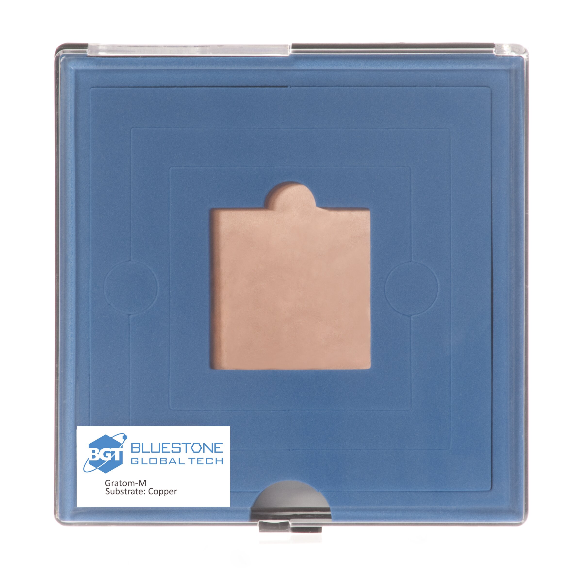
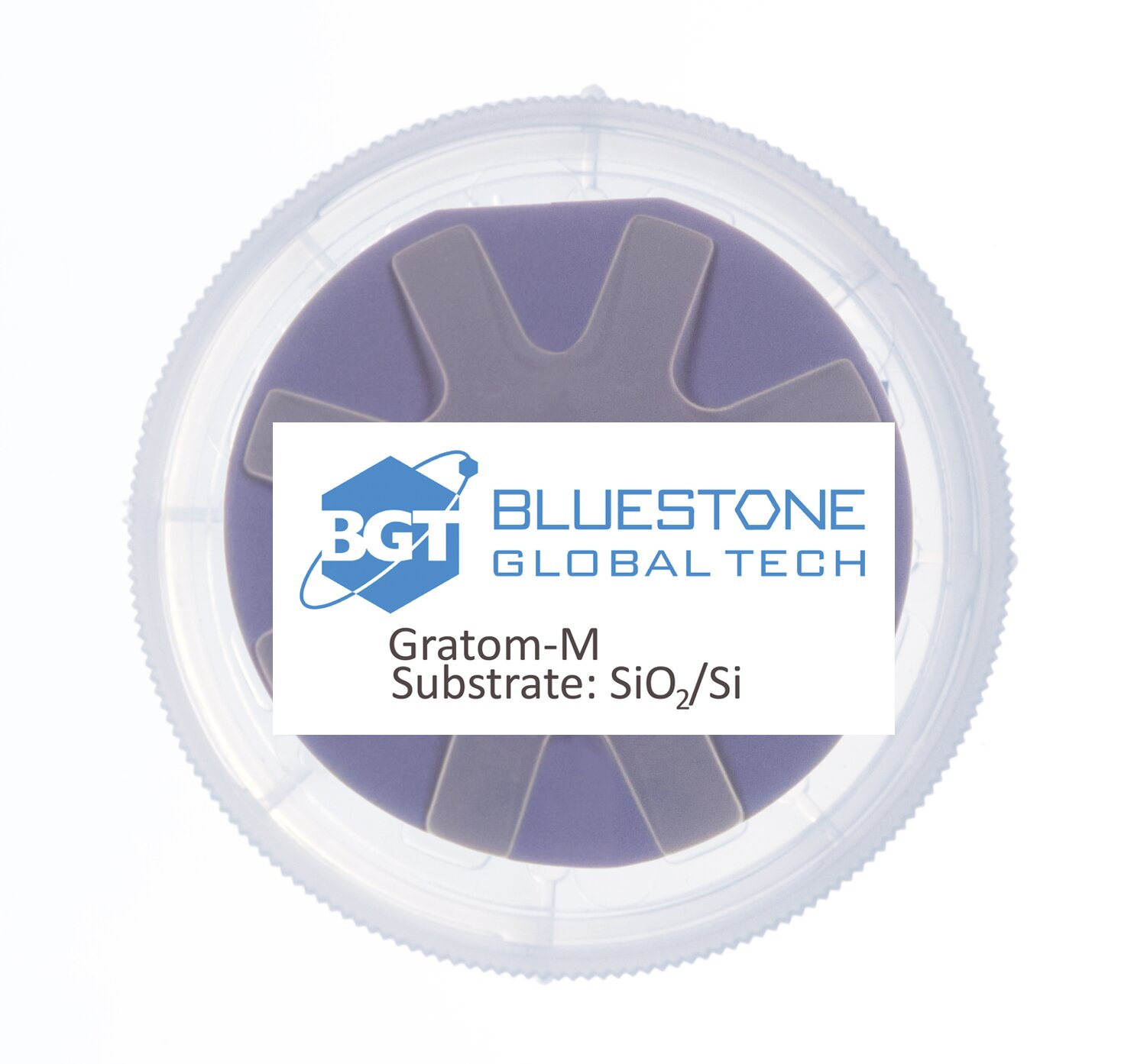
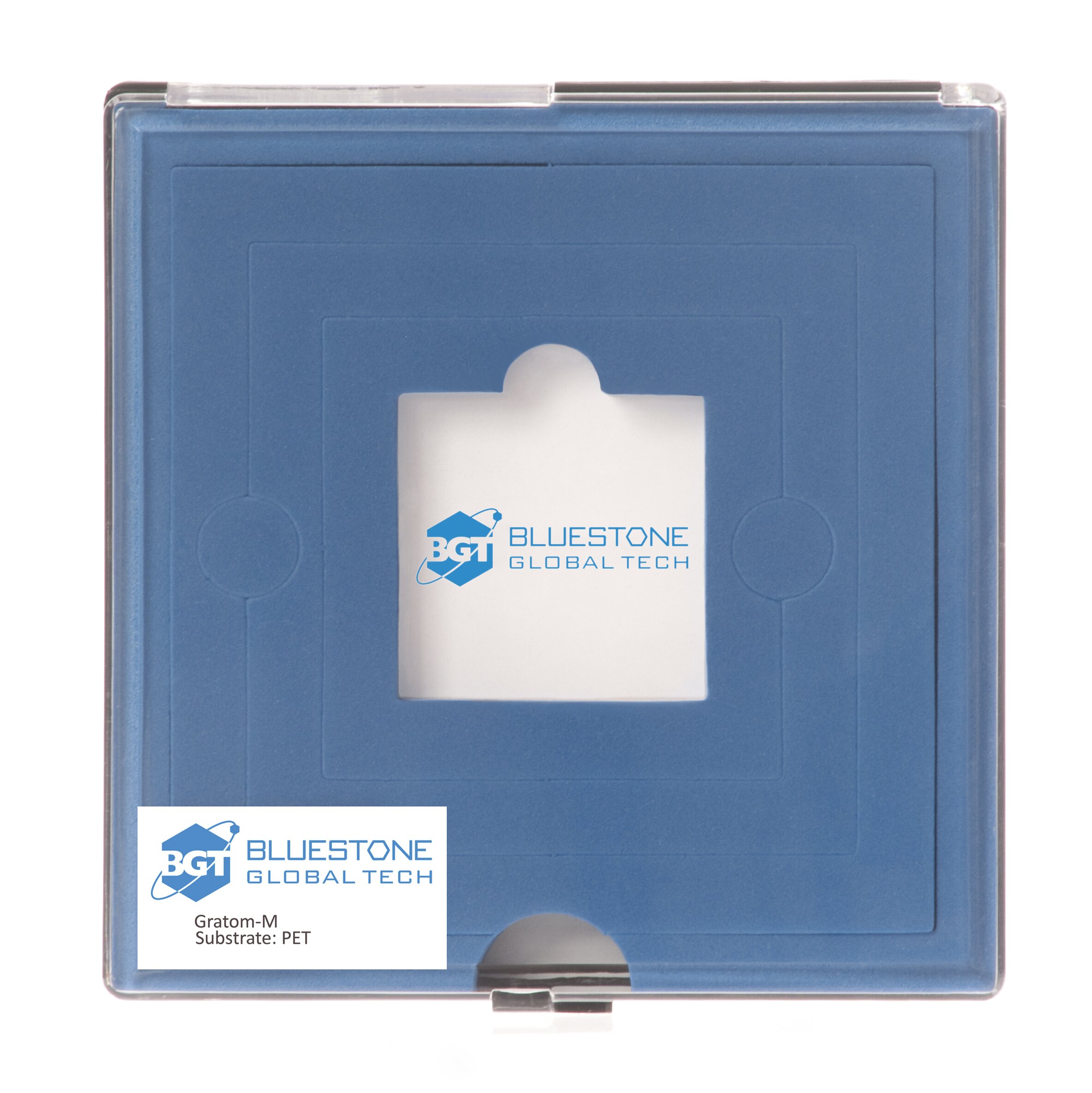
Available on various substrates including Copper, SiO2 and PET, in a range of sizes and defining characteristics, the high-quality of our CVD graphene, Grat-Film, is unparalleled. For an in-depth look at our CVD graphene offerings, please explore our product comparison tables below.   CVD Graphene on Copper

 Product Name Product Features Available Sizes (in2)
Gratom-M-Cu
  • Monolayer percentage > 95%
  • Optical transmittance at 550 nm > 97% (excl. substrate)
  • Average Raman Id/Ig < 5% within domain
  • Average Hall mobility of 2000-4000 cm2/Vs at n=1e12 /cm2
  • Average sheet resistance of 300-600 ohm/sq.
2 x 2

4 x 4

8 x 10

12 x 14

Gratom-R-Cu
  • Monolayer with occasional multilayer islands
  • Optical transmittance at 550 nm > 95% (excl. substrate)
  • Average sheet resistance of 300-600 ohm/sq.
8 x 10

12 x 14

Gratom-A-Cu
  • Large-area, as-grown CVD graphene
12 x 60

24 x 60

24 x 100

24 x 300

Gratom-S-Cu
  • Isolated single graphene domain
  • Large graphene domain (30 – 200 µm)
  • Average Raman Id/Ig < 5% within domain
2 x 2

*Copper thickness 1mil (25 µm)  CVD Graphene on SiO2/Si

Product Name Product Features Available Sizes
Gratom-M-Si1
  • Graphene film coverage > 95% with occasional holes and cracks (< 5 %)
  • Monolayer graphene percentage > 95%
  • # of cracks or holes larger than 3 mm: 0
  • Average Raman Id/Ig < 5% within domain
  • Average Hall mobility of 2000-4000 cm2/Vs at n=1e12 /cm2
  • Average sheet resistance of 300-600 ohm/sq.
1cm x 1cm

2” or 4” wafer

Gratom-M-Si2
  • Graphene film coverage > 99% with occasional holes and cracks (< 1 %)
  • Monolayer graphene percentage > 95%
  • # of cracks or holes larger than 3 mm: 0
  • Average Raman Id/Ig < 5% within domain
  • Average Hall mobility of 2000-4000 cm2/Vs at n=1e12 /cm2
  • Average sheet resistance of 300-600 ohm/sq.
1cm x 1cm

2” or 4” wafer

Gratom-S-Si
  • Isolated single graphene domain
  • Large graphene domain (30 – 200 µm)
  • Average Raman Id/Ig < 5% within domain
2” wafer

*Wafer spec: thermal grown 285-nm SiO2 on p-type Si substrate (resistivity <0 .005 ohm-cm) CVD Graphene transferred on PET

Product Name Product Features Available Sizes (in2)
Gratom-O1
  • Transmission of graphene at 550 nm: > 95% (excl. substrate)
  • Average sheet resistance: < 800 ohm/sq.
2 x 2

4 x 4

8 x 10

Gratom-O2
  • Transmission of graphene at 550 nm: > 95% (excl. substrate)
  • Average sheet resistance: < 300 ohm/sq.
2 x 2

4 x 4

8 x 10

Gratom-O3
  • Transmission of graphene at 550 nm: > 93% (excl. substrate)
  • Average sheet resistance: < 150 ohm/sq.
2 x 2

4 x 4

8 x 10

Gratom-O4
  • Transmission of graphene at 550 nm: > 90% (excl. substrate)
  • Average sheet resistance: < 70 ohm/sq.
2 x 2

4 x 4

8 x 10

Gratom-O5
  • Transmission of graphene at 550 nm: > 85% (excl. substrate)
  • Average sheet resistance: < 30 ohm/sq.
2 x 2

4 x 4

8 x 10

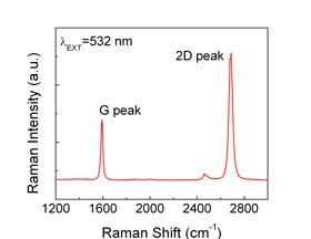
*PET thickness 5 mil (125 micron), transmittance  87% @ 550 nm Complete characterizationTransmittance and uniformity (optical image) Crystallinity (Raman spectroscopy) Sheet resistance (four-probe measurement) Doping density and carrier mobility (Hall effect)

Our high-quality graphene products on Copper, SiO2/Si and PET.

DSC_5886_Gratom_M_Substrate_Copper     DSC_5932a_Gratom_M_Si02_Si     DSC_5886_Gratom_M_Substrate_PET

ALL PRODUCTS CAN BE CUSTOM-MADE ON VIRTUALLY ANY SUBSTRATE AND/OR TO YOUR IDEAL PRODUCT SPECIFICATIONS.